No edit summary Tag: rte-wysiwyg |
|||
| (34 intermediate revisions by 14 users not shown) | |||
| Line 2: | Line 2: | ||
| − | + | A [[chip package]] is what surrounds the [[integrated circuit die]] and connects the die's pads to the packages external pins. They are often a chip carriers, or IC packages. |
|
| Line 8: | Line 8: | ||
=Types of Leads/Contacts= |
=Types of Leads/Contacts= |
||
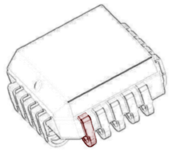
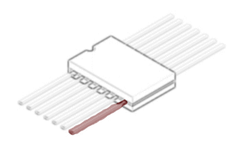
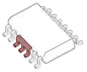
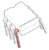
| + | The pieces of metal that electrically connect the IC to a circuit board are called leads. |
||
| − | * J-Lead |
||
| + | |||
| − | * Gull-wing Lead |
||
| + | {| |
||
| − | * C-Bend Lead |
||
| + | | [[Image:Ic leads-j-lead.png|thumb|none|100px|J-Lead]] |
||
| − | * I-Lead |
||
| + | | [[Image:Ic leads-gull wing.png|thumb|none|100px|Gull-wing]] |
||
| − | * Bat-wing Lead |
||
| + | | [[Image:Ic leads-c lead.png|thumb|none|100px|C-Bend]] |
||
| − | * Through-Hole Lead |
||
| + | |- |
||
| − | * Exposed Pad |
||
| + | | [[Image:Ic leads-i lead.png|thumb|none|100px|I-Lead]] |
||
| − | * Ball (solder ball) |
||
| + | | [[Image:Ic leads-batwing.png|thumb|none|100px|Bat-wing ]] |
||
| − | * Tab (Heatsink) |
||
| + | | [[Image:Ic leads-through-hole.png|thumb|none|100px|DIP Through-Hole ]] |
||
| − | * Land pad (Non-leaded/No-lead) |
||
| + | |- |
||
| ⚫ | |||
| + | | [[Image:Ic_leads-exposed_pad.png|thumb|none|100px|Exposed Pad]] |
||
| ⚫ | |||
| + | | [[Image:Ic leads-solder ball.png|thumb|none|100px|Ball (solder ball)]] |
||
| + | | [[Image:Ic leads-Heat-tab.jpg|thumb|none|100px|Tab (Heatsink)]] |
||
| + | |- |
||
| + | | [[Image:Ic leads-pad.png|thumb|none|100px|Land pad (Non-leaded/No-lead)]] |
||
| ⚫ | |||
| ⚫ | |||
| + | |} |
||
=Common Packages= |
=Common Packages= |
||
| Line 25: | Line 32: | ||
* CPGA: Ceramic pin grid array |
* CPGA: Ceramic pin grid array |
||
* PDIP: Plastic dual in-line package |
* PDIP: Plastic dual in-line package |
||
| − | * BGA |
+ | * BGA : Ball grid array |
| − | * SO: Small outline |
+ | * SO: Small outline |
| − | ** SOIC: Small outline |
+ | ** SOIC: Small outline integrated circuit |
| − | ** SOT |
+ | ** SOT: Small outline transistor |
| + | ** SOJ: Small outline J-lead |
||
* PQFP: Plastic quad flat package |
* PQFP: Plastic quad flat package |
||
* PLCC: plastic leaded chip carrier |
* PLCC: plastic leaded chip carrier |
||
* TO: transistor outline |
* TO: transistor outline |
||
| − | |||
| − | |||
| − | |||
=Chip packages= |
=Chip packages= |
||
| Line 50: | Line 55: | ||
*[[Howto identify chip packages/Pin grid array|Pin grid array]] |
*[[Howto identify chip packages/Pin grid array|Pin grid array]] |
||
| − | * PGA |
+ | ** PGA |
*[[Howto identify chip packages/Small outline package|Small outline package]]: |
*[[Howto identify chip packages/Small outline package|Small outline package]]: |
||
| Line 71: | Line 76: | ||
*[[Howto identify chip packages/Quad package|Quad package]] |
*[[Howto identify chip packages/Quad package|Quad package]] |
||
**QFP |
**QFP |
||
| + | **HQFP |
||
*[[Howto identify chip packages/Leadless package|Leadless package]] |
*[[Howto identify chip packages/Leadless package|Leadless package]] |
||
| Line 101: | Line 107: | ||
*[[Howto identify chip packages/Unsorted|Unsorted]] |
*[[Howto identify chip packages/Unsorted|Unsorted]] |
||
| + | ''See all chip package images: [[:Category:Chip package image]]'' |
||
=Chip Carrier Related Acronyms= |
=Chip Carrier Related Acronyms= |
||
| − | * COL: Chip-on-Lead |
+ | * COL: Chip-on-Lead |
| − | * TEP: Top Exposed Pad |
+ | * TEP: Top Exposed Pad |
* EP, EXP: Exposed pad |
* EP, EXP: Exposed pad |
||
* L, LD: Lead |
* L, LD: Lead |
||
| − | * SiP: System in Package |
+ | * SiP: System in Package |
* JEDEC: Joint Electron Device Engineering Council |
* JEDEC: Joint Electron Device Engineering Council |
||
* JEITA: Japan Electronics and Information Technology Industries Association |
* JEITA: Japan Electronics and Information Technology Industries Association |
||
| Line 115: | Line 122: | ||
* Sn: tin |
* Sn: tin |
||
* Cu: Copper |
* Cu: Copper |
||
| − | * |
+ | * Au: Gold |
* EIA: Electronic Industries Alliance |
* EIA: Electronic Industries Alliance |
||
| − | * MCP: |
+ | * MCP: Multi-Chip Package |
* EIAJ: Electronic Industries Association of Japan |
* EIAJ: Electronic Industries Association of Japan |
||
* TAB: Tape Automated Bonding |
* TAB: Tape Automated Bonding |
||
| − | |||
=See Also= |
=See Also= |
||
| Line 128: | Line 134: | ||
* [http://tsc.jeita.or.jp/tsc/standard/downloadE.html JEITA package standards downloads] |
* [http://tsc.jeita.or.jp/tsc/standard/downloadE.html JEITA package standards downloads] |
||
* http://www.standardics.nxp.com/packaging/package.outlines/ |
* http://www.standardics.nxp.com/packaging/package.outlines/ |
||
| − | *http://www.nxp.com/package/ |
+ | * http://www.nxp.com/package/ |
| − | * http://www.analog.com/ |
+ | * http://www.analog.com/en/corporate/quality-and-reliability/packages/index.html |
| + | * |
||
| − | + | *http://www.amkor.com/products/productfamilies.cfm |
|
* http://acronyms.thefreedictionary.com/ |
* http://acronyms.thefreedictionary.com/ |
||
=New links= |
=New links= |
||
| − | *http://www.talkingelectronics.com/projects/CircuitTricks/CircuitTricks-1.html |
+ | *[http://www.talkingelectronics.com/projects/CircuitTricks/CircuitTricks-1.html some chip package desc] |
| − | * GOOD: http:// |
+ | * GOOD: [http://ww1.microchip.com/downloads/en/EnvironmentalInformation/en026304.pdf] |
| ⚫ | |||
| − | * GOOD: http://ww1.microchip.com/downloads/en/EnvironmentalInformation/en026304.pdf |
||
| ⚫ | |||
| ⚫ | |||
| ⚫ | |||
| ⚫ | |||
| ⚫ | |||
| + | * [http://www.napakgd.com/previous/kgd2001/pdf/6-2_Chen.pdf Package in package] |
||
| ⚫ | |||
| − | |||
| ⚫ | |||
*http://www.educypedia.be/electronics/componentfabricationchip.htm |
*http://www.educypedia.be/electronics/componentfabricationchip.htm |
||
| Line 153: | Line 159: | ||
*[http://www.rohm.com/products/databook/pack/pdf/index-e.html ROHM] |
*[http://www.rohm.com/products/databook/pack/pdf/index-e.html ROHM] |
||
* [http://www.sony.co.jp/~semicon/PKG/english/ic.html Sony] |
* [http://www.sony.co.jp/~semicon/PKG/english/ic.html Sony] |
||
| + | *[http://www.ti.com/sc/docs/package/guide.htm TI- long list of names] |
||
| + | * [http://www.pcmag.com/encyclopedia_term/0,2542,t=chip+package&i=39645,00.asp some names] |
||
| + | *[http://www.toplinecomponents.com/SMDnomen.pdf SMD components] |
||
| + | * http://www.fpga-guide.com/package/package.html |
||
| + | * [http://www.google.com/search?hl=en&client=firefox-a&rls=org.mozilla%3Aen-US%3Aofficial&hs=hLz&q=tsqfp+pdf&btnG=Search SMD Dictionary] |
||
| + | * [http://www.esilicon.com/capabs/capPakBGA.htm BGA Packages] |
||
| + | * [http://www.2ic.cn/bbs/viewthread.php?tid=287902 very long list of names] |
||
| + | * [http://www.upv.es/amiga/198.htm list of names] (Spanish) |
||
| + | * [http://www.toshiba.com/taec/components/Generic/LSIpack.pdf BGA side profiles] |
||
| + | * [http://www.engr.sjsu.edu/mjones/LSIpack.pdf BGA side profiles] |
||
| + | * [http://www.esilicon.com/capabs/capPakBGA.htm BGA side profiles] |
||
=completed= |
=completed= |
||
| − | *http://www.analog.com/Analog_Root/Packages/Packages_Home/0,2299,1,00.html |
+ | * [http://www.analog.com/Analog_Root/Packages/Packages_Home/0,2299,1,00.html Analog devices] |
| − | *http://www.amkor.com/ |
+ | * [http://www.amkor.com/ Amkor Technology] |
| − | *http://www.fairchildsemi.com/packaging/ |
+ | * [http://www.fairchildsemi.com/packaging/ Fairchild] |
| − | *''[[Howto identify chip packages/old|old packages]]'' |
+ | *''[[Howto identify chip packages/old|old packages]]''<div id="wikia-credits"><br /><br /><small>From [http://howto.wikia.com HowTo Wiki], a [http://www.wikia.com Wikia] wiki.</small></div> |
| + | [[Category:Howto]] |
||
| + | [[Category:Electronics]] |
||
Latest revision as of 09:39, 28 April 2015
A chip package is what surrounds the integrated circuit die and connects the die's pads to the packages external pins. They are often a chip carriers, or IC packages.
Types of Leads/Contacts
The pieces of metal that electrically connect the IC to a circuit board are called leads.
 J-Lead |
 Gull-wing |
 C-Bend |
  I-Lead |
  Bat-wing |
  DIP Through-Hole |
  Exposed Pad |
  Ball (solder ball) |
  Tab (Heatsink) |
  Land pad (Non-leaded/No-lead) |
PGA Pin | Column |
Common Packages
- CPGA: Ceramic pin grid array
- PDIP: Plastic dual in-line package
- BGA : Ball grid array
- SO: Small outline
- SOIC: Small outline integrated circuit
- SOT: Small outline transistor
- SOJ: Small outline J-lead
- PQFP: Plastic quad flat package
- PLCC: plastic leaded chip carrier
- TO: transistor outline
Chip packages
- In-line package
- DIP
- SIP
- ZIP
- Optical package
- Photodiode
- LED
- IR
- Photo interrupt
- Pin grid array
- PGA
- Small outline package:
- SO
- SOP
- SOIC
- SOT
- SC
- Ball grid array
- BGA
- CSP
- Micro-array
- MicroSMD
- CGA: Column grid array
- Quad package
- QFP
- HQFP
- Leadless package
- QFN
- SON
- LGA
- J-lead package
- SOJ
- LCC
- 2 lead package
- Diodes
- DO
- SOD
- Resistors
- Capacitors
- inductors
- Diodes
- I-lead package
- CERPACK
- CERQUAD
- QFI
- SOI
See all chip package images: Category:Chip package image
Chip Carrier Related Acronyms
- COL: Chip-on-Lead
- TEP: Top Exposed Pad
- EP, EXP: Exposed pad
- L, LD: Lead
- SiP: System in Package
- JEDEC: Joint Electron Device Engineering Council
- JEITA: Japan Electronics and Information Technology Industries Association
- SoC: System on Chip
- ASIC: Application specific Integrated circuit
- Pb: lead
- Sn: tin
- Cu: Copper
- Au: Gold
- EIA: Electronic Industries Alliance
- MCP: Multi-Chip Package
- EIAJ: Electronic Industries Association of Japan
- TAB: Tape Automated Bonding
See Also
External Links
- JEITA package standards downloads
- http://www.standardics.nxp.com/packaging/package.outlines/
- http://www.nxp.com/package/
- http://www.analog.com/en/corporate/quality-and-reliability/packages/index.html
- http://www.amkor.com/products/productfamilies.cfm
New links
- some chip package desc
- GOOD: [1]
- [2]
- ALL ee words: chip-abbreviations
- package names
- NEC
- Intersil
- ROHM
- Sony
- TI- long list of names
- some names
- SMD components
- http://www.fpga-guide.com/package/package.html
- SMD Dictionary
- BGA Packages
- very long list of names
- list of names (Spanish)
- BGA side profiles
- BGA side profiles
- BGA side profiles